What Is A Snubber Circuit?
Key Takeaway
A snubber circuit is used to protect electronic components, like diodes and transistors, from voltage spikes. These spikes can occur during switching operations. The snubber circuit consists of a resistor and capacitor connected in series. When a voltage spike happens, the snubber circuit absorbs and dissipates the excess energy. This prevents damage to the components and ensures the circuit operates smoothly. By controlling the voltage spikes, snubber circuits enhance the reliability and lifespan of electronic devices.
Definition and Function of Snubber Circuits
Snubber circuits are essential components in electrical engineering, used to protect sensitive components from voltage spikes and transients. For newly joined engineers, understanding snubber circuits is crucial for designing robust and reliable electronic systems. This guide will explore the definition, types, applications, design, advantages, and limitations of snubber circuits, providing a comprehensive overview.
A snubber circuit is an electrical circuit used to suppress (snub) voltage spikes and transients in power electronics. These voltage spikes are typically generated when switching devices, such as transistors or thyristors, are turned off. The primary function of a snubber circuit is to absorb these spikes, thereby protecting the switching devices from damage and improving the overall reliability of the system. Snubber circuits are commonly used in power supplies, inverters, motor drives, and other applications where high-speed switching is required.
Types of Snubber Circuits
There are several types of snubber circuits, each designed to address specific issues related to voltage spikes and transients:
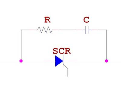
RC Snubber: This type consists of a resistor (R) and a capacitor (C) connected in series. RC snubbers are commonly used to reduce voltage spikes and oscillations in power electronics. They are simple to design and effective in many applications.
RCD Snubber: An extension of the RC snubber, the RCD snubber adds a diode (D) in parallel with the resistor and capacitor. This configuration helps to clamp the voltage and provides better protection for the switching device by allowing the capacitor to discharge rapidly.
LC Snubber: This type uses an inductor (L) and a capacitor (C) to form a low-pass filter, which can effectively suppress high-frequency oscillations. LC snubbers are used in applications where inductive loads are present, such as motor drives.
TVS Diode Snubber: Transient Voltage Suppression (TVS) diodes are used to clamp voltage spikes to a safe level. TVS diodes are fast-acting and provide excellent protection against transient events.
Each type of snubber circuit has its advantages and is selected based on the specific requirements of the application.
Applications of Snubber Circuits
Snubber circuits are used in a wide range of applications to protect sensitive components and improve the performance of electronic systems:
Power Supplies: In switch-mode power supplies (SMPS), snubber circuits protect switching transistors from voltage spikes, ensuring reliable operation and extending the lifespan of the components.
Motor Drives: In motor control systems, snubber circuits suppress voltage spikes generated by inductive loads, preventing damage to the switching devices and reducing electromagnetic interference (EMI).
Inverters: Snubber circuits are used in inverters to protect the switching devices from transients, improving the efficiency and reliability of the power conversion process.
Relays and Contactors: Snubber circuits are used to suppress voltage spikes generated when relays and contactors open and close, preventing damage to the contacts and reducing arcing.
High-Frequency Circuits: In high-frequency circuits, snubber circuits help to dampen oscillations and improve signal integrity.
The versatility of snubber circuits makes them indispensable in various electronic and electrical applications.
How to Design and Implement a Snubber Circuit
Designing and implementing a snubber circuit involves several steps:
Identify the Problem: Determine the source and nature of the voltage spikes or transients that need to be suppressed. This could involve analyzing the circuit and identifying the switching devices that generate the spikes.
Select the Snubber Type: Choose the appropriate type of snubber circuit based on the application and the specific requirements. For instance, RC snubbers are suitable for general-purpose applications, while RCD snubbers provide better clamping.
Calculate Component Values: Calculate the values of the snubber components (resistor, capacitor, inductor) based on the voltage, current, and frequency characteristics of the circuit. This typically involves using formulas and guidelines specific to the type of snubber being used.
Implement the Snubber: Integrate the snubber circuit into the design, ensuring proper placement and connections. This may involve adding the snubber components across the switching device or load.
Test and Optimize: Test the circuit to ensure that the snubber is effectively suppressing the voltage spikes. Adjust the component values if necessary to achieve optimal performance.
Proper design and implementation of snubber circuits are crucial for ensuring the protection and reliability of electronic systems.
Advantages and Limitations of Snubber Circuits
Snubber circuits offer several advantages, including:
Protection of Components: Snubber circuits protect sensitive switching devices from voltage spikes, reducing the risk of damage and extending the lifespan of the components.
Improved Reliability: By suppressing voltage transients, snubber circuits enhance the overall reliability and stability of electronic systems.
Reduced EMI: Snubber circuits help to reduce electromagnetic interference by damping oscillations and suppressing high-frequency noise.
However, there are also limitations to consider:
Component Size and Cost: Adding snubber circuits increases the size and cost of the overall design, which may be a concern in space-constrained or cost-sensitive applications.
Power Dissipation: Snubber circuits can dissipate power, which may reduce the efficiency of the system. Proper design is needed to minimize power loss.
Complexity: Designing and tuning snubber circuits can be complex, requiring careful analysis and optimization to achieve the desired performance.
Conclusion
Snubber circuits play a crucial role in protecting electrical components from voltage spikes and transients, enhancing the reliability and performance of electronic systems. For newly joined engineers, understanding the different types of snubber circuits, their applications, and how to design and implement them is essential. Despite their limitations, the benefits of snubber circuits in safeguarding sensitive components and ensuring stable operation make them indispensable in modern electronics. By mastering the principles of snubber circuits, engineers can design robust systems that withstand the challenges of high-speed switching and harsh electrical environments.